
The TC4953ES is an 11 V P‑channel enhancement MOSFET with low on‑resistance and high ESD protection.
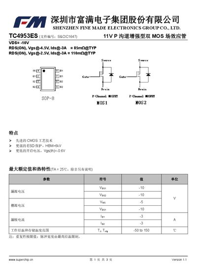
The TC4953ES is a P‑channel enhancement MOSFET fabricated with advanced CMOS technology. It offers strong ESD protection (HBM > 6 kV) and a low gate‑threshold voltage of –0.6 V.
Key electrical ratings include a maximum drain‑source voltage of –10 V, a maximum gate‑source voltage of –5 V, and a continuous drain current of –3 A. Typical on‑resistance is 85 mΩ at VGS = –4.5 V and 110 mΩ at VGS = –2.5 V. The device is supplied in an SOP‑8 package. This manual is written in Chinese.
| Maximum Drain‑Source Voltage (VDS) | -10 V |
|---|---|
| Maximum Gate‑Source Voltage (VGS) | -5 V |
| Continuous Drain Current (ID) | -3 A |
| ESD Protection (HBM) | > 6 kV |
| Package | SOP‑8 |
The maximum drain‑source voltage is –10 V.
It provides ESD protection greater than 6 kV (HBM).
The device is supplied in an SOP‑8 package.