
Design guide covering power, clock, I/O, configuration and schematic best‑practice for Gowin GW2A/GW2AR series FPGAs.
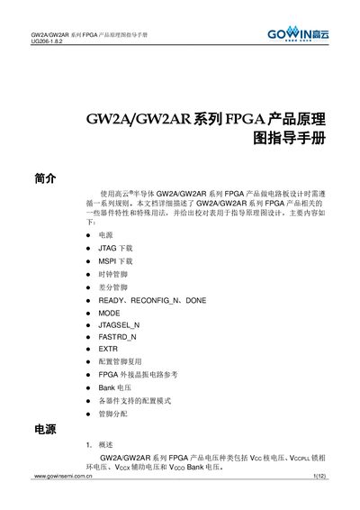
This guide provides detailed design information for the Gowin GW2A/GW2AR series FPGA devices. It describes device characteristics, recommended power supplies, pin assignments, and configuration modes to help engineers create reliable schematics.
Key topics include power‑rail specifications, JTAG and MSPI download interfaces, clock and differential pins, configuration‑signal behavior (READY, RECONFIG_N, DONE, MODE, JTAGSEL_N, FASTRD_N, EXTR), pin‑multiplexing, external crystal oscillator circuits, bank voltage requirements, and supported configuration modes for each device package. This manual is written in Chinese.
| VCC voltage range | 0.95 V – 1.05 V |
|---|---|
| VCCPLL voltage range | 0.95 V – 1.05 V |
| VCCO (I/O Bank) voltage range | 1.14 V – 3.6 V |
| VCCX (auxiliary) voltage range | 2.375 V – 3.6 V |
| Recommended power‑up time | 0.2 ms – 2 ms |
VCC should be 0.95 V–1.05 V, VCCPLL 0.95 V–1.05 V, VCCO 1.14 V–3.6 V, and VCCX 2.375 V–3.6 V.
The power‑up time should be between 0.2 ms and 2 ms; if longer than 2 ms, VCC must come up before VCCX/VCCO.