
This guide provides schematic design information for Gowin GW1NZ series FPGA, covering power, clock, JTAG, MSPI, pin assignments and configuration modes.
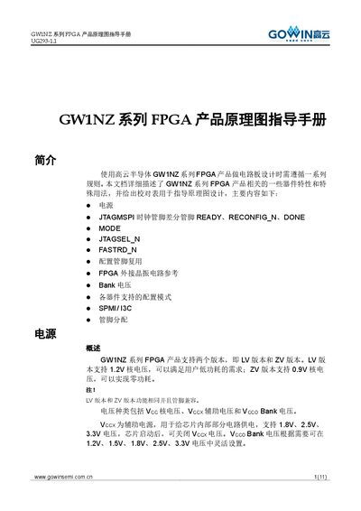
The document describes the GW1NZ series FPGA design rules, including power supply options (LV and ZV versions), recommended voltage ranges, and pin multiplexing. It details the JTAG and MSPI interfaces, clock pin architecture, differential signal standards, and configuration pin behavior such as READY, RECONFIG_N, and DONE.
Additional sections cover the external crystal oscillator circuit, SPMI/I3C interfaces, pin assignment strategies, and configuration pin reuse. Technical support contact information and revision history are provided at the end of the guide. This manual is written in Chinese.
| VCC (LV version) voltage range | 1.14 V – 1.26 V |
|---|---|
| VCC (ZV version) voltage range | 0.88 V – 1.00 V |
| VCCO (I/O Bank) voltage range | 1.14 V – 3.6 V |
| VCCX (auxiliary) voltage range | 1.71 V – 3.6 V |
The LV version requires 1.14 V to 1.26 V, while the ZV version requires 0.88 V to 1.00 V.
READY must be high for the FPGA to be configurable; if it is low, a power‑up or RECONFIG_N pulse is needed to restore configuration capability.
Yes, after configuration the pins can be set to GPIO, but their initial states must be set correctly (e.g., RECONFIG_N high, DONE high) to ensure proper operation.