
Datasheet for the Fairchild FDW2502P dual P-channel 2.5V specified PowerTrench MOSFET with -20 V rating, 35 mΩ on-resistance and TSSOP-8 package.
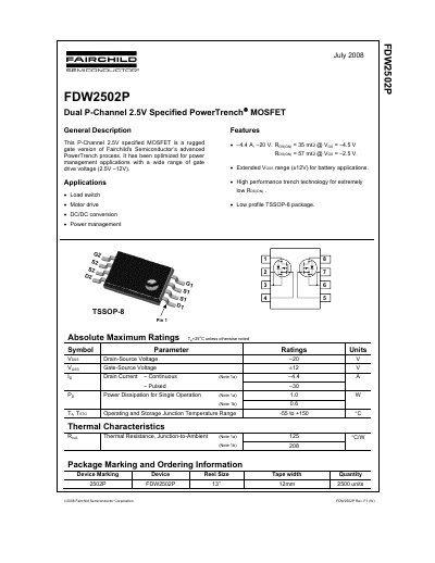
This datasheet from Fairchild Semiconductor describes the FDW2502P, a dual P-channel MOSFET specified for 2.5V gate drive. The device is built on Fairchild's PowerTrench process and is intended for power management applications over a gate drive voltage range of 2.5V to 12V. It is rated at -4.4 A and -20 V, with an extended gate-source voltage range of ±12V for battery applications.
The document lists the device applications (load switch, motor drive, DC/DC conversion and power management), absolute maximum ratings, thermal characteristics, package marking and ordering information, full electrical characteristics, and typical performance curves for on-resistance, transfer, body diode, gate charge, capacitance, safe operating area and transient thermal response. The FDW2502P comes in a low profile TSSOP-8 package and is supplied on a 13 inch reel with 12 mm tape, 2500 units per reel.
| Drain-Source Voltage (VDSS) | -20 V |
|---|---|
| Gate-Source Voltage (VGSS) | ±12 V |
| Drain Current - Continuous | -4.4 A (Note 1a) |
| Pulsed Drain Current | -30 A |
| Power Dissipation, Single Operation | 1.0 W (Note 1a), 0.6 W (Note 1b) |
| Operating and Storage Junction Temperature Range | -55 to +150 °C |
| Thermal Resistance, Junction-to-Ambient | 125 °C/W on 1 inch² copper pad; 208 °C/W on minimum copper pad |
| Static Drain-Source On-Resistance at VGS = -4.5 V | 35 mΩ |
| Static Drain-Source On-Resistance at VGS = -2.5 V | 57 mΩ |
| Input Capacitance (Ciss) | 1465 pF |
| Total Gate Charge (Qg) | 15 nC typical, 21 nC maximum |
| Package | TSSOP-8 |
| Ordering Information | 2500 units per reel, 13 inch reel, 12 mm tape |
The drain-source voltage rating (VDSS) is -20 V.
RDS(ON) is 35 mΩ at VGS = -4.5 V.
It is supplied in a low profile TSSOP-8 package.
The listed applications are load switch, motor drive, DC/DC conversion and power management.