
The Fairchild CD4007C datasheet provides specifications, pin assignments, and usage limits for the dual complementary pair plus inverter MOS IC.
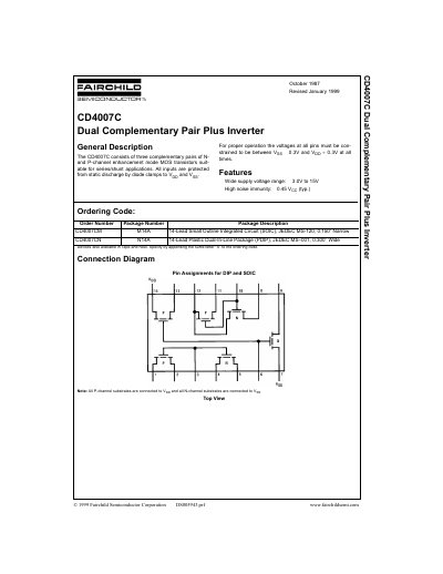
The CD4007C is a CMOS integrated circuit that contains three complementary N‑ and P‑channel MOS transistor pairs, suitable for series and shunt applications. All inputs are protected from static discharge by diode clamps to VDD and VSS, and the device operates over a wide supply voltage range.
The document lists absolute maximum ratings, DC and AC electrical characteristics, package dimensions for both SOIC and PDIP versions, and a life‑support policy stating the component is not authorized for critical medical use without explicit approval.
| Supply voltage range | 3.0 V to 15 V |
|---|---|
| Noise immunity (VNH) | 3.6 V at VDD=5 V, 7.0 V at VDD=10 V |
| Operating temperature range | -40 °C to +85 °C |
| Power dissipation (PD) – DIP | 700 mW |
| Input leakage current (II) | 10 pA |
| Propagation delay (tPLH) at VDD=5 V | 35 ns (min) – 75 ns (max) |
| Input capacitance (CI) | 5 pF |
The device operates with a supply voltage from 3.0 V up to 15 V.
It can operate between –40 °C and +85 °C.
The DIP (PDIP) package can dissipate up to 700 mW.
No, Fairchild does not authorize its use in life‑support devices without written approval.