
This datasheet details the specifications, features, and applications of the AD5304, AD5314, and AD5324 quad buffered voltage output DACs from Analog Devices.
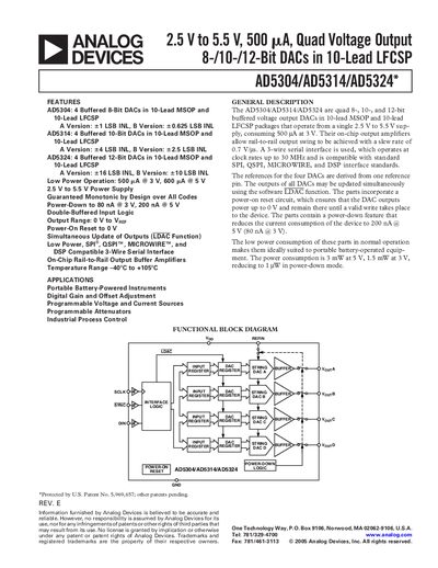
The AD5304/AD5314/AD5324 are quad 8-, 10-, and 12-bit buffered voltage output DACs available in 10-lead MSOP and LFCSP packages. They operate from a single 2.5 V to 5.5 V supply and consume low power, making them suitable for portable battery-powered instruments. The devices feature on-chip rail-to-rail output buffer amplifiers and a 3-wire serial interface compatible with SPI, QSPI, MICROWIRE, and DSP standards.
| Resolution | 8, 10, or 12 Bits |
|---|---|
| Power Supply Range | 2.5 V to 5.5 V |
| Supply Current (Normal) | 500 µA @ 3 V |
| Power-Down Current | 80 nA @ 3 V |
| Operating Temperature | -40 °C to +105 °C |
| Output Voltage Range | 0 V to V REF |
| Interface Compatibility | SPI, QSPI, MICROWIRE, DSP |
The typical supply current is 500 µA at 3 V.
The power-down current is 200 nA at 5 V.
Yes, the outputs are guaranteed monotonic by design over all codes.