
DC919A is a demonstration circuit produced by Linear Technology for 16-bit/14-bit 10Msps to 105Msps ADCs.
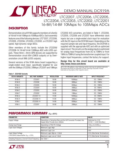
This document provides setup and operation instructions for the DC919A demonstration circuit, which supports a family of high-speed ADCs. The board includes variants for different ADC models and sample rates, optimized for analog input frequencies from DC to 70MHz. It features a single-ended clock input and supports both differential and single-ended input configurations. The manual details jumper settings, power requirements, clock input specifications, and data collection using the DC718 QuikEval II system or logic analyzers.
The board is designed for evaluating ADC performance with tools like PScope software. It includes circuitry optimized for various input frequencies and supports transformer-coupled or direct DC input paths. Users are advised to use low-jitter clock sources and may need to modify the board for specific applications such as undersampling or higher-frequency inputs. This manual is written in Chinese.
| Supply Voltage | 3.3V [3.15V ↔ 3.45V Min/Max] |
|---|---|
| Logic Input Voltage | Minimum Logic High 2.4V, Maximum Logic Low 0.8V |
| Logic Output Voltage | Minimum Logic High at –1.6mA 2.3V, Maximum Logic Low at 1.6mA 0.7V |
| Sampling Frequency | See Table 1 |
| Input Frequency Range | DC to 70MHz |
The DC919A supports LTC2207, LTC2206, LTC2205, LTC2204, LTC2203, LTC2202, and LTC2201 ADCs.
The maximum sampling rate is 105Msps for the LTC2207 and LTC2207-14 variants.
A low jitter 3.3V oscillator with direct connection through a barrel is recommended.
The DC919A requires up to 500mA and must be powered with 3.3V across the pins marked “+3.3V” and “PWR GND”.