
DC1766A is a low phase noise, dual CMOS output buffer/driver/logic converter
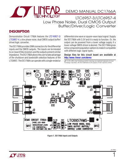
This manual provides instructions for operating the DC1766A demo board, which features the LTC6957-3/LTC6957-4 low phase noise dual CMOS output buffer/driver/logic converter. It includes setup procedures, configuration options, and assembly variations for different output types. The board supports both single-ended and differential input signals and allows bandwidth selection and output shutdown via jumpers. It is designed for engineering development and evaluation purposes only, not for commercial use.
The manual also includes a parts list, schematic diagram, and layout recommendations for optimal performance. Safety and handling precautions are emphasized, including electrostatic discharge protection and the need for electronics training. The board is supplied with 3.3V and can operate with a lower voltage supply for CMOS output if needed.
| Input Type | Single-ended or differential sine wave or square-wave |
|---|---|
| Supply Voltage | 3.3V (default) or 2.4V–3.3V (for lower voltage CMOS output) |
| Output Type | In-Phase CMOS (DC1766A-A) or Complementary CMOS (DC1766A-B) |
| Input Impedance | 50Ω |
| Output Impedance | 50Ω |
| Output Coupling | AC-coupled |
The DC1766A is supplied with 3.3V by default.
Use jumper VDD (JP7) at the V+ position for 3.3V output, or move it to EXT position and apply 2.4V–3.3V between VDD (E4) and GND (E3) for lower voltage output.
DC1766A-A provides In-Phase CMOS output using LTC6957HMS-3, and DC1766A-B provides Complementary CMOS output using LTC6957HMS-4.
The DC1766A is a demonstration board for evaluating the LTC6957-3/LTC6957-4 low phase noise dual CMOS output buffer/driver/logic converter.