
This document is the user manual of DC2425A, which introduces the characteristics and usage methods of DC2425A
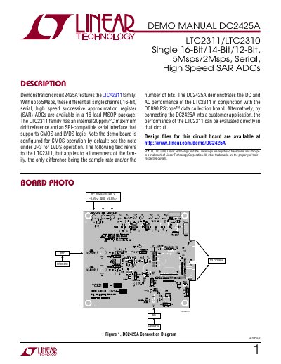
This document is a demonstration manual for the DC2425A circuit board, which features the LTC2311 family of differential, single channel, 16-bit serial high speed successive approximation register (SAR) ADCs. The board is designed to demonstrate the DC and AC performance of the LTC2311 in conjunction with the DC890 PScope data collection board or for direct evaluation in customer applications.
The manual provides a quick start procedure for connecting the board to a host PC and running the PScope software. It details various hardware setup options, including signal connections for differential and single-ended inputs, clock requirements, and jumper configurations for power supply selection, reference sources, and data output formats.
| ADC Family | LTC2311 family |
|---|---|
| Resolution | 16-bit/14-bit/12-bit |
| Sample Rate | Up to 5Msps |
| Package | 16-lead MSOP |
| Reference Drift | 20ppm/°C maximum |
| Clock Frequency (Max) | 105MHz |
| Clock Frequency (Max) | 42MHz |
| Clock Jitter Requirement | Under 2ps |
| Default VCCIO | 2.5V |
| Default VDD | 5V |
| Default Reference Source | DRIVE REFOUT |
The maximum conversion rate depends on the specific assembly version, ranging from 2Msps to 5Msps.
Use jumper JP1 to select the VCCIO supply voltage, with default settings at 2.5V and an option for 1.8V.
The default setting is DRIVE REFOUT, which uses the voltage applied to Pin 3 of the LTC2311 as the reference voltage.
Yes, the DC2425A is capable of accepting a single-ended signal as well as a differential input signal.