
The TL103W and TL103WA combine the building blocks of a dual operational amplifier and a fixed voltage reference - both of which are often used in the control circuitry of both switch-mode and linear power supplies. OPAMP1 has its noninverting input internally tied to a fixed 2.5-V reference, while OPAMP2 is independent, with both inputs uncommitted. For the A grade, especially tight voltage regulation can be achieved.
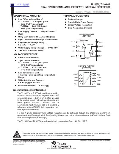
The TL103W and TL103WA combine the building blocks of a dual operational amplifier and a fixed voltage reference, designed for use in control circuitry for switch-mode and linear power supplies. OPAMP1 has its noninverting input internally tied to a fixed 2.5-V reference, while OPAMP2 is independent with both inputs uncommitted. The A grade offers especially tight voltage regulation with low offset voltages and tight tolerances for the voltage reference.
These devices are characterized for operation from -40°C to 105°C and are available in SOIC and QFN packages. Key features include a low supply current of 350 µA/channel (typical), a unity gain bandwidth of 0.9 MHz (typical), and a wide output voltage swing from OV to VCC - 1.5 V. The internal voltage reference provides a fixed 2.5-V output with a tolerance of 0.4% at 25°C for the A grade.
| Offset Voltage (A Grade) | 3 mV (25°C) and 5 mV (Full Temperature) |
|---|---|
| Offset Voltage (Standard Grade) | 4 mV (25°C) and 5 mV (Full Temperature) |
| Supply Current | 350 µA/Channel (Typ) |
| Unity Gain Bandwidth | 0.9 MHz (Typ) |
| Supply Voltage Range | 3 V to 32 V |
| Reference Voltage Tolerance (A Grade) | 0.4% (25°C) and 0.8% (Full Temperature) |
| Reference Voltage Tolerance (Standard Grade) | 0.7% (25°C) and 1.4% (Full Temperature) |
| Operating Temperature Range | -40°C to 105°C |
| Output Sink Current | 0.5 mA (Typ) to 100 mA |
Typical applications include battery chargers, switch-mode power supplies, linear voltage regulation, and data-acquisition systems.
The device includes a fixed 2.5-V reference voltage.
The maximum junction temperature is 150°C.