
The TS615 is a dual operational amplifier featuring a high output current 410mA, which can be configured differentially for driving signals in telecommunication systems using multiple carriers. The TS615 is ideally suited for xDSL (High Speed Asymmetrical Digital Subscriber Line) applications. This circuit is capable of driving a 10Ω or 25Ω load at ±2.5V, 5V, ±6V or +12V power supply. The TS615 will be able to reach a -3dB bandwidth of 40MHz on 25Ω load with a 12dB gain. This device is designed for the high slew rates to support low harmonic distortion and inter-modulation. The TS615 is fitted out with Power Down function to decrease the consumption. During this sleep state the device displays a short circuit output in order to keep the impedance matching with the line. The TS615 is housed in TSSOP14 Exposed-Pad plastic package for a very low thermal resistance.
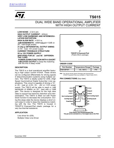
The TS615 is a dual operational amplifier designed with a high output current of 420mA and a low noise level of 2.5nV/VHz. It features a current feedback structure and is specified for differential loads of 200 and 50 ohms. The device includes a power-down function that maintains a short-circuited output to ensure impedance matching with the line during sleep mode.
This amplifier is ideally suited for xDSL (High Speed Asymmetrical Digital Subscriber Line) applications and can drive 10 or 25 ohm loads at various power supply voltages. It is housed in a TSSOP14 Exposed-Pad plastic package to provide very low thermal resistance. Key performance metrics include a slew rate of 410V/us and a -3dB bandwidth of 40MHz.
| Low Noise | 2.5nV/VHz |
|---|---|
| High Output Current | 420mA |
| High Slew Rate | 410V/us |
| -3dB Bandwidth | 40MHz |
| Power Supply Range | 5V to 12V |
| Package Type | TSSOP14 Exposed-Pad |
| Operating Temperature | -40 to +85 °C |
| Equivalent Input Noise Voltage | 25 nV/VHz |
The TS615 is ideally suited for xDSL (High Speed Asymmetrical Digital Subscriber Line) applications.
The device displays a short-circuited output during sleep mode to keep impedance matching with the line.
The maximum junction temperature is 150 °C.