
The MM54C914-MM74C914 is a monolithic CMOS Hex Schmitt trigger with a special input protection scheme. This scheme allows the input voltage levels to exceed VCC or ground by at least 10V (VCC ≤ 25V to GND ≥ 25V), which is valuable for applications involving voltage level shifting or mismatched power supplies. The positive and negative-going threshold voltages, VTa and VTb, show low variation with respect to temperature (typ 0.0005V/°C at VCC = 10V), and the hysteresis, VTa - VTb ≥ 0.2 VCC, is guaranteed.
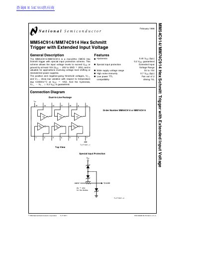
The document describes the MM54C914/MM74C914, a monolithic CMOS Hex Hysteresis Schmitt trigger with special input protection. This scheme allows input voltages to exceed Vcc by at least 10V (from -25V to +25V relative to ground), making it valuable for voltage level shifting and mismatched power supply applications.
| Operating Voltage Range (Vcc) | 3V to 15V |
|---|---|
| Operating Temperature Range (MM74C914) | -40°C to +85°C |
Input pins can withstand voltages from -25V to +25V relative to ground, while other pins range from -0.3V to Voc + 0.3V.