
This document introduces a series of logic gate products, including Quad 2-Input NAND Gate, Quad 2-Input NOR Gate, Hex Inverter, Triple 3-Input NAND Gate, and Dual 4-Input NAND Gate. These products use complementary MOS (CMOS) technology and have wide power supply operating range, low power consumption, high noise immunity, and symmetric controlled rise and fall times. The 54C-74C logic family is functionally and pin compatible with the 54-74 series devices, minimizing design time for designers familiar with the standard 54-74 logic family. All inputs are protected from damage due to static discharge by diode clamps.
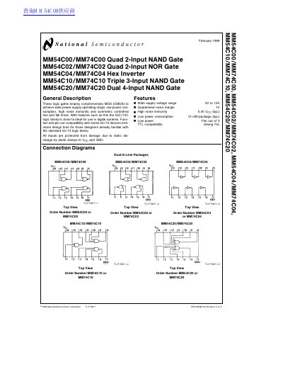
This document is a technical data sheet for the National Semiconductor MM54C00/MM74C00 family of CMOS logic gates. The series includes quad 2-input NAND gates, quad 2-input NOR gates, hex inverters, triple 3-input NAND gates, and dual 4-input NAND gates. These devices utilize complementary MOS technology to offer a wide power supply operating range (3V to 15V), low power consumption, and high noise immunity. They are functionally and pin-compatible with the standard 54/74 logic series.
| Operating VCC Range | 3.0V to 15V |
|---|---|
| Maximum VCC Voltage | 18V |
| Power Dissipation (Dual-In-Line) | 700 mW |
| Power Dissipation (Small Outline) | 500 mW |
| Typical Power Consumption | 10 nW/package |
| Propagation Delay Time (VCC=5.0V) | 50 ns |
The guaranteed operating voltage range is 3V to 15V.
Yes, they offer function and pin out compatibility with the series 54/74 devices.
The typical power consumption is 10 nW per package.