
This application note describes the functionality and how the STSR3 device can be used as the secondary synchronous rectifier driver in Flyback topology switched mode power supplies. A schematic and layout description of a demo board that is able to replace diode rectification with synchronous rectification in Flyback converters is shown below.
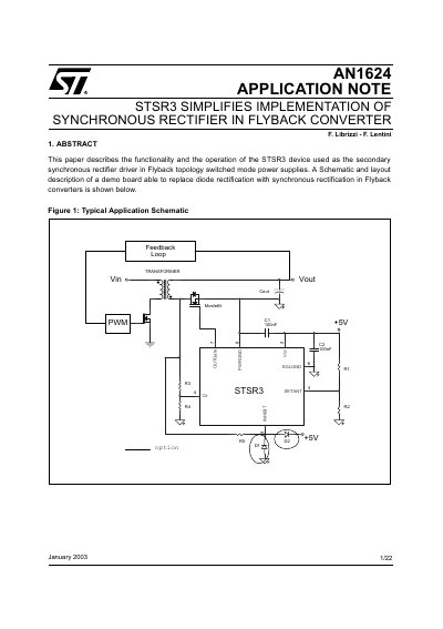
This document details the functionality and operation of the STSR3 device, which acts as a secondary synchronous rectifier driver for high-efficiency Flyback topology switched mode power supplies. It explains how the IC generates driving signals with set dead times based on a synchronizing clock input to prevent shoot-through conditions.
| Supply Input Range | 4V to 5.5V |
|---|---|
| Maximum Driving Voltage | 5.5V |
| Package Type | SO-8 |
| Internal Zener Limit | 5.8V |
The INHIBIT pin acts as a Discontinuous Mode Detector that allows shut-off of the drive output by sensing the Synchronous Rectifier source-drain voltage.
The STSR3 obtains synchronization directly from the secondary side using the voltage across the Synchronous mosfet as the information for the switching transitions.