
This application note reports on the design of a 2 kW-100 V, 123 MHz Class AB peak power amplifier (PPA) for 3 Tesla MRI applications. It almost doubles the output power of previous amplifiers using MOSFET transistors in standard ceramic packages. The design techniques and construction practices are described in enough detail to permit duplication of the amplifier.
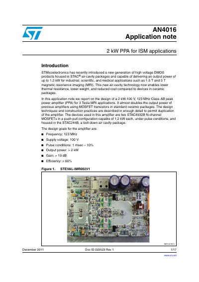
The document details the design of a 2 kW, 100 V, 123 MHz Class AB peak power amplifier (PPA) intended for industrial, scientific, and medical applications such as 3 Tesla MRI. The design utilizes two STAC4932B N-channel MOSFETs in a push-pull configuration housed in STAC air cavity packages to achieve high output power with lower thermal resistance compared to ceramic packages.
The amplifier design prioritizes compactness (100 x 150 mm), full surface-mount technology, and the avoidance of ferromagnetic components. It employs planar microstrip technology for RF circuits, including embedded transformers T1 and T2 on the PCB substrate. The input network uses a balun transformer and power splitters to ensure electrical symmetry, while the output network utilizes an impedance transformer to manage high DC current and optimize impedance.
| Frequency | 123 MHz |
|---|---|
| Supply voltage | 100 V |
| Pulse conditions | 1 msec — 10% |
| Output power | > 2 kW |
| Gain | > 19 dB |
| Efficiency | > 60% |
The amplifier operates at a frequency of 123 MHz with a supply voltage of 100 V.
The device operates under pulse conditions of 1 msec with a duty cycle of 10% and delivers an output power greater than 2 kW.
The design requires a gain of more than 19 dB and an efficiency exceeding 60%.