
This document describes the AD9286 evaluation board, which provides all of the support circuitry required to evaluate the functionality of the AD9286 analog-to-digital converter. The evaluation board features full-featured support for setup and control via the SPI interface, supports LVDS output mode options, provides external or on-board oscillator options, supports balun/transformer or amplifier input drive options, and includes switching power supplies. It can be operated using the VisualAnalog and SPIController software interfaces.
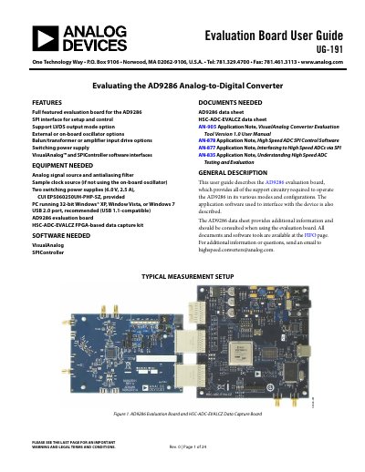
This document provides instructions for the AD9286 evaluation board, which includes all necessary support circuitry to operate the device in various modes. It details the equipment and software required, such as the VisualAnalog and SPIController interfaces, and describes the typical measurement setup involving signal sources and data capture kits.
The guide covers hardware configuration, including power supply connections, analog input settings, and clock circuitry options. It explains how to configure jumpers for different analog input modes, enabling separate clocking, or non-SPI operation, and provides a quick start procedure for using the accompanying software.
| Analog Input Frequency | up to ~200 MHz |
|---|---|
| Reference Voltage | 1.0 V |
| RBIAS Default Setting | 10 kΩ |
| Power Supply Output | 6 V, 2 A |
The required software includes VisualAnalog and SPIController.
Write a value 0 to SPI Address 0x09 and place a jumper across J204 to tie AUXCLKEN to DRVDD.
Remove the shorting jumpers on J302 to disconnect CSB, SCLK, and SDIO/PWDN pins from the SPI control bus.