
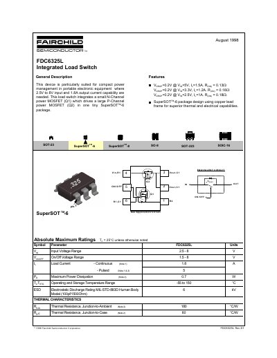
The FDC6325L from Fairchild Semiconductor is an integrated load switch intended for compact power management in portable electronic equipment where 2.5 V to 8 V input and 1.8 A output current capability are needed. It integrates a small N-Channel power MOSFET (Q1) that drives a large P-Channel power MOSFET (Q2) in one SuperSOT-6 package.
This datasheet gives the absolute maximum ratings, thermal characteristics and electrical characteristics of the device, including conduction voltage drop and static on-resistance at 5 V, 3.3 V and 2.5 V input. It also shows a load switch application circuit, recommends external components R1, R2 and C1 for slew rate and in-rush current control, and presents typical electrical characteristics curves and a transient thermal response curve. The document is dated August 1998 and is revision Rev.D1.
| Input Voltage Range | 2.5 V to 8 V |
|---|---|
| On/Off Voltage Range | 1.5 V to 8 V |
| Load Current, Continuous | 1.8 A |
| Load Current, Pulsed | 5 A |
| Maximum Power Dissipation | 0.7 W |
| Operating and Storage Temperature Range | -55 to 150 °C |
| Electrostatic Discharge Rating | 6 kV (MIL-STD-883D Human Body Model, 100 pF/1500 ohm) |
| Thermal Resistance, Junction-to-Ambient | 180 °C/W |
| Thermal Resistance, Junction-to-Case | 60 °C/W |
| Package | SuperSOT-6 |
The input voltage range is 2.5 V to 8 V, with an on/off voltage range of 1.5 V to 8 V.
The continuous load current is 1.8 A and the pulsed load current is 5 A.
It is supplied in a SuperSOT-6 package that integrates the N-Channel and P-Channel power MOSFETs.
The datasheet states that users can download a "FDC6325L.MOD" SPICE model from the Fairchild web site at www.fairchildsemi.com.