
This document provides information about the absolute maximum ratings and electrical characteristics of the MMBF5103 semiconductor device produced by Fairchild Semiconductor Corporation. The document includes the operating and storage temperature range of the device, as well as parameters related to the static and dynamic characteristics of the device. This includes maximum voltage ratings, maximum current ratings, breakdown voltage, input capacitance, and output capacitance.
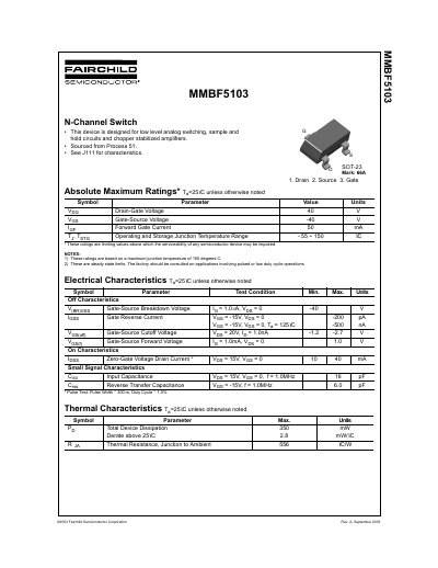
This document provides the design specifications for the MMBF5103, an N-Channel Switch designed for low-level analog switching, sample and hold circuits, and chopper stabilized amplifiers. The device is sourced from Process 51 and is available in the SOT-23 package.
| Drain-Gate Voltage | 40 V |
|---|---|
| Gate-Source Voltage | -40 V |
| Forward Gate Current | 50 mA |
| Operating Junction Temperature Range | -55 ~ 150 °C |
| Total Device Dissipation | 350 mW |
| Thermal Resistance, Junction to Ambient | 556 °C/W |
It is designed for low level analog switching, sample and hold circuits and chopper stabilized amplifiers.
This device is designed for low level analog switching, sample and hold circuits, and chopper stabilized amplifiers.
The operating and storage junction temperature range is from -55 to 150 degrees Celsius.
The maximum total device dissipation is 350 milliwatts.