
The R3200x Series are reset timer ICs with two input signals for mobile equipments which require long interval for reset sequence. The long interval prevents unexpected resets caused by accidental key operations. Internally, each of these ICs consist of a delay generator circuit and output driver transistors. The R3200x Series have two active-low input pins (SR0 and SR1) which generate reset signals after output delay time when both input pins are activated at the same time. R3200x Series has two versions that are different in output delay time settings and output release method. - R3200x001x : Output delay time selectable (7.5s or 11.25s) by connecting DSR pin to either GND or VDD. The reset signal will be canceled if either of the input pin becomes “H”. Until either input pin becomes “H”, the reset signal will be continually outputted. - R3200x002x : Output delay time is fixed at 7.5s. After the reset signal is being output 0.234s, it will be released automatically or if either of the input pin becomes “H”, the reset signal will be canceled. While the reset signals are remaining active or being sent out, the ICs provide ultra-low supply current. The R3200x Series are available in DFN(PLP)2020-8B and DFN1216-8 packages.
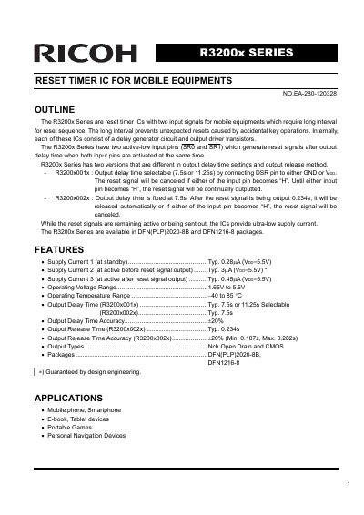
The Ricoh R3200x Series consists of reset timer integrated circuits designed for mobile equipment that require long intervals for reset sequences to prevent unexpected resets from accidental key operations. These ICs feature two active-low input pins (SRO and SR1) which generate a reset signal after a specific output delay time when both are activated simultaneously.
The series is available in two versions with different configurations: the R3200x001x version allows selectable output delay times of 7.5s or 11.25s via an external pin connection, while the R3200x002x version has a fixed 7.5s delay time. Both versions offer ultra-low supply current during reset signal activity and are available in DFN(PLP)2020-8B and DFN1216-8 packages.
| Operating Voltage Range | 1.65V to 5.5V |
|---|---|
| Operating Temperature Range | -40 to 85 °C |
| Output Delay Time (R3200x001x) | 7.5s or 11.25s Selectable |
| Output Delay Time (R3200x002x) | Fixed at 7.5s |
| Output Release Time (R3200x002x) | Typ. 0.234s |
| Output Types | Nch Open Drain and CMOS |
The ICs are suitable for mobile phones, smartphones, e-books, tablet devices, portable games, and personal navigation devices.
The delay time is selectable by connecting the DSR pin to either GND (for 7.5s) or Voo (for 11.25s).
If either of the input pins (SRO or SR1) becomes 'H', the reset signal will be canceled immediately.