
This product is a low-power MOSFET from Motorola, model P3
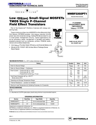
This document provides technical data for the MMBF2202PT1, a miniature surface-mount P-channel enhancement-mode MOSFET designed for power management applications. Utilizing Motorola's High Density TMOS process, this device features low on-resistance to minimize power loss and conserve energy in portable products such as computers, printers, and telephones.
The datasheet details maximum ratings, electrical characteristics including static and dynamic parameters, switching times, and source-drain diode specifications. It also includes information for using the SC-70/SOT-323 surface mount package, recommended board footprints, soldering precautions to prevent thermal stress, and mechanical package dimensions.
| Drain-to-Source Voltage (Vdss) | 20 Vdc |
|---|---|
| Gate-to-Source Voltage (Vgs) | +/- 20 Vdc |
| Continuous Drain Current @ 25°C (Ib) | 300 mA |
| Pulsed Drain Current (Idm) | 750 mA |
| Total Power Dissipation @ 25°C (Pd) | 150 mW |
| Operating Temperature Range (Tj/Tstg) | -55 to 150 °C |
| Thermal Resistance Junction-to-Ambient (RθJA) | 833 °C/W |
| Static Drain-to-Source On-Resistance (Vgs=10V, Id=200mA) | 2.2 Ohms |
| Package Type | SC-70/SOT-323 |
Typical applications are dc-dc converters and power management in portable and battery-powered products such as computers, printers, PCMCIA cards, cellular and cordless telephones.
The soldering temperature and time shall not exceed 260°C for more than 10 seconds.
The maximum operating and storage temperature range is from -55 to 150 °C.