
This is a document generated by ICminer.com Electronic-Library Service.
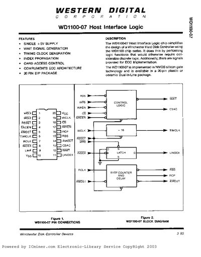
The WD1100-07 is a Host Interface Logic chip designed to simplify the design of Winchester Hard Disk Controllers using the WD1100 chip series. Implemented in NMOS silicon gate technology, it is available in a 20-pin plastic or ceramic Dual-in-Line package. The chip performs logic functions such as timing clock generation, index propagation, and ECC architecture support that would otherwise require discrete logic components.
| Package Type | 20-pin plastic or ceramic Dual-in-Line |
|---|---|
| Ambient Temperature (Operating) | 0°C to 50°C |
| Storage Temperature (Plastic) | -55°C to +125°C |
| WCLK Frequency | 6.25 MHz |
The WAIT output goes true when the controller is internally accessing data or has not accepted data from the host during a WRITE.
TIMCLK is a divided by sixteen version of the WCLK input signal.
LINDEX is a delayed version of the INDEX input and remains high until reset by the LINR input.