
This is a PDF file with Powered by ICminer.com Electronic-Library Service CopyRight 2003 Powered by ICminer.com Electronic-Library Service CopyRight 2003 Powered by ICminer.com Electronic-Library Service CopyRight 2003 Powered by ICminer.com Electronic-Library Service CopyRight 2003 content
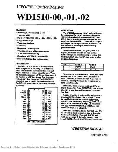
The WD1510 buffer register provides dual‑port asynchronous operation, allowing data to be written to one port and read from the other, or to function as a LIFO using a single port. Word length can be set to 128 or 132 words, and the device includes EMPTY and FULL status flags.
Electrical characteristics include a 5 V supply, TTL‑compatible inputs and outputs, and timing parameters such as a 400 ns master reset time and 550 ns data‑valid window. The pinout defines separate chip‑select lines for each port, a direction pin to control data flow, and status pins for buffer state.
| Word length selectable | 128 or 132 words |
|---|---|
| Word width | 9 bits |
| Maximum data rate | 1.5 MHz (WD1510‑02) |
| Supply voltage | 5 V only |
| TTL compatibility | TTL compatible on all inputs and outputs |
| Package | 28‑pin plastic or ceramic DIP |
| Input leakage current | 10 pA |
| Input high voltage | 2.2 V |
| Input low voltage | 0.8 V |
| Output high voltage | 2.4 V |
| Power‑supply current (typical) | 125 µA |
| Master reset time | 400 ns |
| Data valid from CS | 550 ns |
The device can be configured for either 128‑word or 132‑word depth.
The DIRECTION pin (pin 25) determines the direction: high selects Port A write/Port B read, low selects the opposite.
The chip operates on a 5‑volt supply only and does not require an external clock.