
CLC111 is a high performance, closed loop, monolithic buffer designed by National Semiconductor for applications requiring very high frequency signals. This device's high performance includes an extremely fast 800MHz small signal bandwidth (0.5pp) and an ultra high (3500V/µs) slew rate while requiring only 10.5mA quiescent current. Signal fidelity is maintained with low harmonic distortion (−62dBc 2nd and 3rd harmonics at 20MHz). These performance characteristics are for a demanding 100Ω load. Featuring a patented closed loop design, the CLC111 offers nearly ideal unity gain (0.996) with a very low (1.4Ω) output impedance. The CLC111 is ideally suited for buffering video signals with its 0.15%/0.04˚ differential gain and phase performance at 4.43MHz. Power sensitive applications will benefit from the CLC111's excellent performance on reduced or single supply voltages. Constructed using an advanced, complementary bipolar process and National Semiconductor's proven high performance architectures, the CLC111 is available in several versions to meet a variety of requirements. Enhanced Solutions (Military/Aerospace) SMD Number: contact factory Space level versions also available. For more information, visit http://www.national.com/mil.
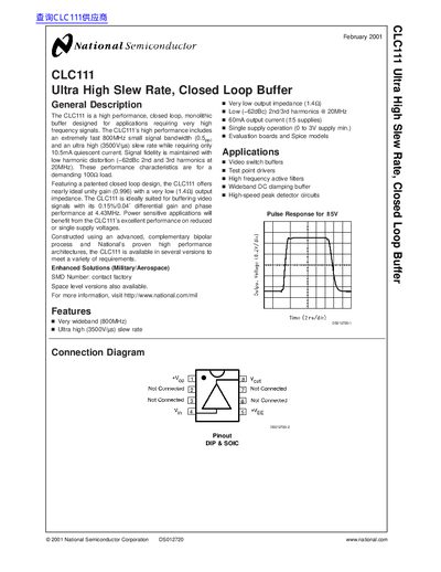
The CLC111 is a monolithic buffer designed for demanding applications requiring very high frequency signals. Key performance characteristics include an extremely fast small signal bandwidth of 800MHz, an ultra-high slew rate of 8500V/us, and low harmonic distortion (-62dBc at 2nd and 3rd harmonics). The device operates with a quiescent current of only 10.5mA.
| Small Signal Bandwidth (Vout < 0.5Vpp) | 800 MHz |
|---|---|
| Slew Rate | 8500 V/us |
| Quiescent Current | 10.5 mA |
| 2nd Harmonic Distortion (at 20MHz) | -62 dBc |
| Output Resistance | 1.4 Ohms |
| Operating Temperature Range | -40°C to +85°C |
The device can operate with a single supply voltage as low as 0V, provided the other terminal is at 3V.
The device operates within a range of -40°C to +85°C.