
The ADP3110 is a dual high voltage MOSFET driver optimized for driving two N-channel MOSFETs, which are the two switches in a nonisolated synchronous buck power converter. Each of the drivers is capable of driving a 3000 pF load with a 25 ns propagation delay and a 30 ns transition time. One of the drivers can be bootstrapped and is designed to handle the high voltage slew rate associated with floating high-side gate drivers.
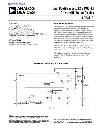
The ADP3110 is an all-in-one synchronous buck driver optimized for driving two N-channel MOSFETs in nonisolated synchronous buck power converters. It features a single PWM signal to generate both high-side and low-side drives, along with anticross-conduction protection circuitry.
| Supply Voltage Range | 4.5 V to 13.2 V |
|---|---|
| Operating Temperature Range | 0°C to 85°C |
| Package Type | 8-lead SOIC_N |
| Load Drive Capability | 3000 pF |
Each driver is capable of driving a 3 nF load.
The low-side MOSFET begins to turn on once the switch node voltage falls to 1 V.
The device operates over an ambient temperature range of 0°C to 85°C.