
The ADP3162 is a highly efficient dual output synchronous buck controller that uses ADOPT™ optimized positioning technology to achieve superior load transient response and the least output capacitors. The ADP3162 complies with VRM 8.5 with the lowest system cost. ADP3162 adopts active current balancing technology to achieve current balancing between two output phases, and provides 5-bit digitally programmable 1.05 V to 1.825 V output and dual logic level PWM outputs for interface to external high-power drivers. The ADP3162 has a total output accuracy of ±0.8% (over temperature), supports current mode operation, provides short circuit protection, power good output, overvoltage protection and undervoltage protection, and does not require other external components to protect the microprocessor.
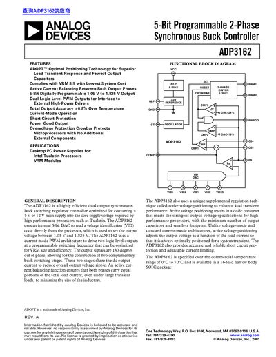
The ADP3162 is a highly efficient dual output synchronous buck switching regulator controller designed to convert a 5 V or 12 V main supply into the core supply voltage required by high-performance processors such as Tualatin. It utilizes an internal 5-bit DAC to read a voltage identification (VID) code directly from the processor, setting the output voltage between 1.05 V and 1.825 V.
The device employs a current mode PWM architecture with active current balancing to ensure both phases carry equal portions of the total load current. It features ADOPT™ Optimal Positioning Technology for superior load transient response and complies with VRM 8.5 specifications.
| Output Voltage Range | 1.05 V to 1.825 V |
|---|---|
| Output Accuracy | +0.8% Over Temperature |
| Operating Ambient Temperature Range | 0°C to 70°C |
| Package Type | 16-lead narrow body SOIC |
| Maximum Oscillator Frequency | 2000 kHz |
The device is optimized for converting supplies to core voltages required by high-performance processors such as Tualatin.
It uses an internal 5-bit DAC to read a voltage identification (VID) code directly from the processor.