
This document describes the features and characteristics of ADuC831, including 8-channel 12-bit ADC, dual 12-bit voltage output DACs, on-chip temperature sensor, and voltage reference. The product also features 62KB flash/EE program memory, 4KB flash/EE data memory, and 2304 bytes of data RAM. It utilizes an 8051 core with support for various peripheral interfaces and power modes. It is suitable for applications such as laser power control in optical networking.
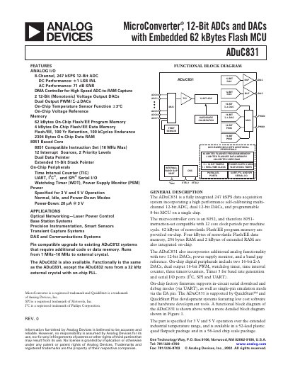
The ADuC831 is a fully integrated MicroConverter featuring an 8‑channel, 247 kSPS, 12‑bit ADC, dual 12‑bit DACs, and an 8051‑compatible MCU core. It includes 62 kB Flash program memory, 4 kB data memory, and 2.3 kB RAM, and operates from 3 V to 5 V across an industrial temperature range.
This datasheet provides a complete description of the device, including functional block diagrams, pin configurations, electrical specifications, timing characteristics, and recommended design considerations for power supply, grounding, and layout. It also lists ordering options and absolute maximum ratings.
| ADC Channels | 8 |
|---|---|
| ADC Sample Rate | 247 kSPS |
| ADC Resolution | 12 bits |
| Flash Program Memory | 62 kBytes |
| Flash Data Memory | 4 kBytes |
| On‑Chip RAM | 2304 Bytes |
| Core Type | 8051‑compatible, up to 16 MHz |
| Operating Voltage | 3 V to 5 V |
The ADuC831 provides an 8‑channel, 12‑bit ADC that can sample at 247 kSPS.
It includes 62 kBytes of on‑chip Flash/EE program memory.
The device is specified for operation at 3 V to 5 V.
It uses an 8051‑compatible core with a maximum clock of 16 MHz.