
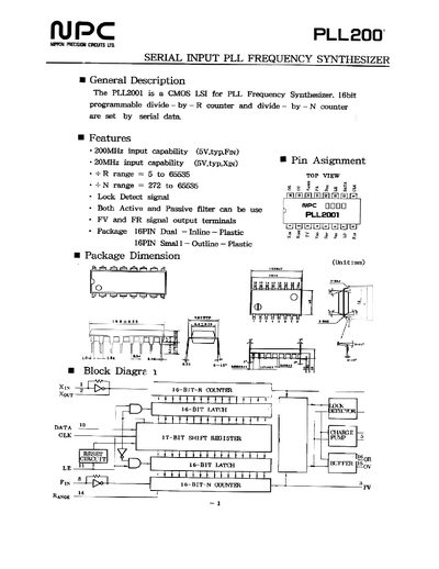
The document describes the PLL200 serial‑input PLL frequency synthesizer, a CMOS LSI device with programmable 16‑bit divide‑R and divide‑N counters. It lists key features such as a 200 MHz input capability, selectable active or passive filters, and various output signals. Pin assignments and detailed pin descriptions are provided, covering inputs like XIN, XOUT, FIN, and control pins such as DATA, CLK, LE, and LD.
Electrical characteristics are given, including supply voltage ranges, current consumption under different operating conditions, and absolute maximum ratings for power supply, input voltage, and temperature. Guidelines for setting divide ratios via serial data and timing requirements for the shift register are also included.
| Input frequency range (high) | 5 MHz to 250 MHz (typ 5.0 V) |
|---|---|
| Input frequency range (low) | DC to 22 MHz (typ 5.0 V) |
| Supply voltage (VDD) | 2.7 V to 5.5 V |
| Current consumption (IDD1L) at FIN=60 MHz | 2.7~3.3 V, 1 Vp‑p sine wave |
| Maximum operating frequency (FIN) high range | 180 MHz |
| Input voltage (VIN) | 2.7 V to 5.5 V |
| Absolute maximum rating – Power Supply VDD | -0.3 V to 0.7 V |
Serial data must be input from the MSB, latched on the rising edge of CLK, while the LE pin is held low during the write operation.
LD is the unlock‑detect terminal; it goes low when the PLL is unlocked.
The device operates with a supply voltage (VDD) between 2.7 V and 5.5 V.