
The LTC1293/4/6 is a family of data acquisition systems which contain a serial I/O successive approximation A/D converter. It uses LTCMOS TM switched capacitor technology to perform either 12-bit unipolar, or 11-bit plus sign bipolar A/D conversions. The input multiplexer can be configured for either single ended or differential inputs (or combinations thereof). An on-chip sample and hold is included for all single ended input channels. When the LTC1293/4/6 is idle it can be powered down in applications where low power consumption is desired. The LTC1296 includes a System Shutdown Output pin which can be used to power down external circuitry, such as signal conditioning circuitry prior to the input mux. The serial I/O is designed to communicate without external hardware to most MPU serial ports and all MPU parallel I/O ports allowing up to eight channels of data to be transmitted over as few as three wires.
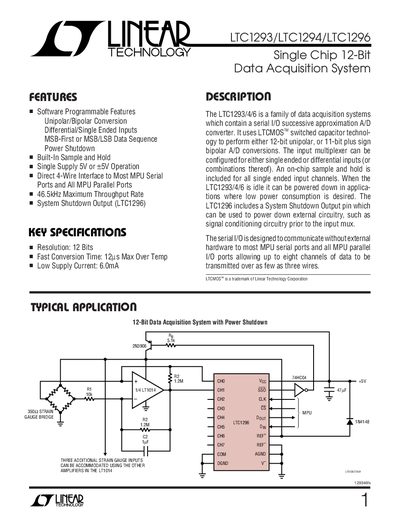
The LTC1293/4/6 family is a single‑chip 12‑bit data acquisition system with programmable unipolar/bipolar conversion, on‑chip sample‑and‑hold, and a 4‑wire serial interface. It supports up to eight analog input channels and includes a system‑shutdown output on the LTC1296 variant.
The document lists key specifications such as resolution, conversion time, supply current, and package options, and provides detailed pin descriptions, electrical characteristics, and typical performance graphs for designers and technicians.
| Resolution | 12 Bits |
|---|---|
| Maximum Throughput Rate | 46.5 kHz |
| Conversion Time | 12 µs |
| Supply Current | 6.0 mA |
| Supply Voltage | Single Supply 5 V |
| Analog Input Range | -0.05 V to VCC + 0.05 V |
The device can achieve a maximum throughput rate of 46.5 kHz.