
The AD9540 is a 655MHz low jitter clock generator from ADI company. It has excellent intrinsic jitter performance, 25Mb/s write-speed serial I/O control, 200MHz phase frequency detector inputs, 655MHz programmable input dividers, programmable RF divider, 8 programmable internal clock rates, 93 fS resolution programmable edge delay, 1.8V power supply, 3.3V power supply, programmable charge pump current, multi-chip synchronization, dual-mode PLL lock detect and 655MHz CML mode PECL compliant driver.
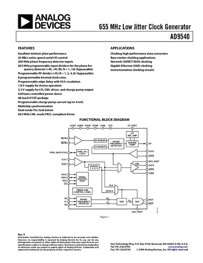
The AD9540 clock generator is designed for high‑performance data‑converter and networking applications, providing a 655 MHz CML‑mode, PECL‑compliant output driver with programmable slew rates. It supports external VCO frequencies up to 2.7 GHz and features a flexible 200 MHz phase‑frequency detector, programmable charge‑pump current, and a 25 Mb/s serial I/O interface.
Key specifications include ultra‑low jitter (720 fs rms for a 105 MHz ADC clock), wide‑range programmable input dividers (M,N = 1‑16), RF divider options (R = 1, 2, 4, 8), and a total power consumption of 400 mW. The device operates over an extended automotive temperature range of –40 °C to +85 °C and is supplied in a 48‑lead LFCSP package.
| Phase Noise @ 10 Hz offset | 80 dBc/Hz |
|---|---|
| Programmable RF Divider | R = 1, 2, 4, 8 (bypassable) |
| External VCO Frequency Range | Up to 2.7 GHz |
| Total Power Consumption (all functions on) | 400 mW |
| Operating Temperature Range | -40 °C to +85 °C |
The AD9540 supports external VCO rates up to 2.7 GHz.
It consumes 400 mW total power with all functions active.
The device operates from –40 °C to +85 °C.
The serial I/O port has a device write‑speed of 25 Mb/s.