
The ADP3118 is a dual high voltage MOSFET driver optimized for driving two N-channel MOSFETs, which are the two switches in a nonisolated synchronous buck power converter. Each of the drivers is capable of driving a 3000 pF load with a 25 ns propagation delay and a 25 ns transition time. One of the drivers can be bootstrapped and is designed to handle the high voltage slew rate associated with the nonisolated synchronous buck power converter.
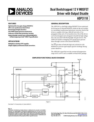
The ADP3118 driver provides optimized low‑gate‑charge MOSFET control for dual N‑channel MOSFETs in non‑isolated synchronous buck converters. It features a single PWM input, bootstrapped high‑side drive, overlapping protection, and an output‑disable pin that floats the output per Intel VRM specifications.
The device operates from a 12 V supply, supports a 0 °C‑85 °C temperature range, and is offered in an 8‑lead SOIC package. Detailed specifications include input voltage thresholds, output resistance values, propagation delays, and timing characteristics for both high‑side and low‑side drivers.
| Input Voltage High | 2.0 V |
|---|---|
| Input Voltage Low | 0.8 V |
| Supply Voltage Range | 4.15 V to 13.2 V |
| Output Resistance (Sourcing, BST‑SW=12 V) | 2.2 Ω to 3.5 Ω |
The device can be powered with a supply voltage between 4.15 V and 13.2 V.
The high‑level PWM input voltage must be at least 2.0 V.