
AD7303 is a dual 8-bit serial input, dual voltage output DAC from Analog Devices. It is available in 8-pin DIP/SOIC and microSOIC packages, and operates from a single +2.7 V to +5.5 V supply. It has an internal reference voltage, individual DAC power-down function, and supports QSPI™, SPI™ and Microwire™ three-wire serial interface. It also has an on-chip output buffer, supports rail-to-rail output, and has low power consumption, with a typical operating current of 2.3 mA and a full power-down current of 1µA. It is suitable for applications such as portable battery powered instruments, digital gain and offset adjustment, programmable voltage and current sources, and programmable attenuators.
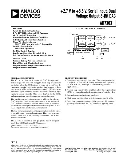
The AD7303 provides two independent 8‑bit DAC channels in a compact 8‑pin DIP, SOIC or micro‑SOIC package. It operates from a single +2.7 V to +5.5 V supply and offers both internal and external reference options, as well as individual power‑down control for each channel.
Its versatile 3‑wire serial interface is compatible with QSPI, SPI and Microwire standards, supporting clock rates up to 30 MHz. The on‑chip output buffers deliver rail‑to‑rail swing with typical 1.2 µs settling time and a slew rate of about 7.5 V/µs, making the device suitable for portable, battery‑powered instruments and programmable voltage sources.
| Resolution | 8 bits |
|---|---|
| Supply Voltage (VDD) | +2.7 V to +5.5 V |
| Output Voltage Range | 0 V to VDD |
| Typical Settling Time | 1.2 µs (max 2 µs) |
| Slew Rate | 7.5 V/µs typ |
| Full‑Power‑Down Current | 80 nA typ |
The device operates from a single supply of +2.7 V to +5.5 V.
In full power‑down the AD7303 typically consumes 80 nA.
The serial interface can operate at clock rates up to 30 MHz.
Yes, each DAC channel has an individual power‑down function.