
The AD9444 is a 14-bit monolithic, sampling analog-to-digital converter (ADC) with an on-chip, track-and-hold circuit. It operates at a guaranteed sampling rate of 80 MSPS and offers excellent linearity, low power dissipation, and support for various applications such as multicarrier, multimode cellular receivers, antenna array positioning, power amplifier linearization, broadband wireless, radar, and infrared imaging.
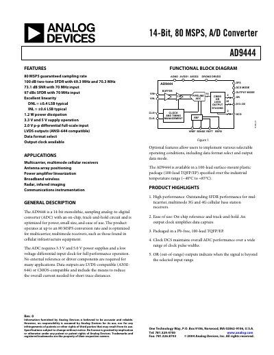
The AD9444 is a 14‑bit monolithic sampling ADC optimized for low power, small size, and ease of use. It operates up to 80 MSPS and supports both LVDS‑compatible (ANSI‑644) and CMOS output formats. The device requires 3.3 V and 5.0 V supplies and a low‑voltage‑differential input clock.
The datasheet provides detailed electrical specifications, pin configurations, timing diagrams, and evaluation board schematics. It also includes absolute maximum ratings, thermal information, and ordering details for the 100‑lead TQFP/EP package.
| Resolution | 14 bits |
|---|---|
| Maximum Sampling Rate | 80 MSPS |
| Supply Voltage AVDD1 | 3.3 V |
| Supply Voltage AVDD2 | 5.0 V |
| Power Consumption (LVDS output) | 1.21 W typical |
| Differential Input Range | 2 V p‑p |
| Differential Nonlinearity (DNL) | ±0.4 LSB |
| Integral Nonlinearity (INL) | ±0.6 LSB |
| Signal‑to‑Noise Ratio (10 MHz) | ≈73 dB |
| Spurious‑Free Dynamic Range (10 MHz) | ≈97 dBc |
| Effective Number of Bits (10 MHz) | 12.1 bits |
The AD9444 can sample at up to 80 MSPS.
The device uses 3.3 V for AVDD1 and 5.0 V for AVDD2.
Typical power consumption is about 1.21 W (up to 1.4 W).
The ADC accepts a 2 V p‑p differential input with a common‑mode voltage of 3.5 V.