
The LTC1483 is an ultra-low power differential line transceiver designed for data transmission standard RS485 applications with extended common-mode range (–7V to 12V). It will also meet the requirements of RS422. The LTC1483 features output drivers with controlled slew rate, decreasing the EMI radiated from the RS485 lines, and improving signal fidelity with misterminated lines. The CMOS design offers significant power savings over its bipolar counterparts without sacrificing ruggedness against overload or ESD damage. Typical quiescent current is only 80µA while operating and less than 1µA in shutdown. The driver and receiver feature three-state outputs, with the driver outputs maintaining high impedance over the entire common-mode range. Excessive power dissipation caused by bus contention or faults is prevented by a thermal shutdown circuit which forces the driver outputs into a high impedance state. The receiver has a fail-safe feature which guarantees a high output state when the inputs are left open. I/O pins are protected against multiple ESD strikes of over ±10kV. The LTC1483 is fully specified over the commercial and extended industrial temperature range and is available in 8-pin DIP and SO packages.
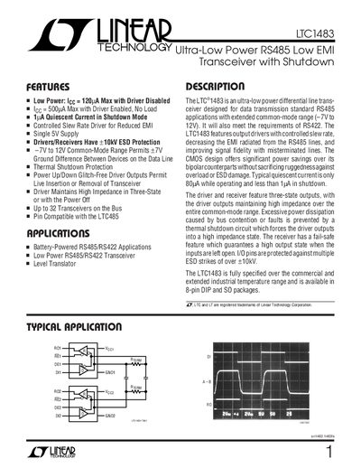
The LTC1483 is an ultra‑low‑power differential line transceiver for RS485 and RS422 applications. It features a controlled slew‑rate driver for reduced EMI, a wide common‑mode range of –7 V to +12 V, and built‑in thermal shutdown and ESD protection. The device operates from a single 5 V supply and is available in 8‑lead DIP and SOIC packages.
The datasheet provides absolute maximum ratings, electrical characteristics, switching times, pin functions, and typical performance graphs. It also includes application information such as low‑power operation, shutdown mode behavior, and recommended test circuits.
| Supply Voltage (VCC) | 5 V |
|---|---|
| Quiescent Current (Driver Enabled) | 120 µA max |
| Shutdown Mode Current | 1 pA |
| Common‑Mode Voltage Range | –7 V to +12 V |
| Maximum Data Rate | 250 kbits/s |
| Package Types | 8‑lead DIP and 8‑lead SOIC |
The LTC1483 supports a maximum data rate of 250 kbits/s.
In shutdown mode the device draws only about 1 pA of supply current.
The transceiver operates over a common‑mode range from –7 V to +12 V.
When the driver is disabled the quiescent current is 120 µA max.