
The LTC3125 is a high effi ciency, synchronous step-up DC/DC converter with an accurate programmable average input current limit. The ±5% accurate average input current is resistor programmable and suitable for a wide variety of applications. In mobile computing, GSM and GPRS cards demand high current pulses well beyond the capability of the PC Card and CompactFlash slots. The LTC3125 in concert with a reservoir capacitor, keeps the slot power safely within its capabilities providing a high performance and simple solution. Synchronous rectifi cation produces high effi ciency while the 1.6MHz switching frequency minimizes the solution footprint. The current mode PWM design is internally com- pensated. Output disconnect allows the load to discharge in shutdown, while also providing inrush current limiting. Other features include a <1μA shutdown current, short- circuit and thermal overload protection. The LTC3125 is of- fered in a low profi le 0.75mm × 2mm × 3mm package.
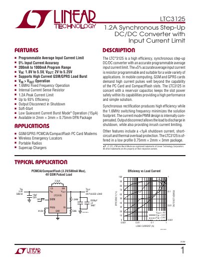
The LTC3125 is a high‑efficiency synchronous boost converter with programmable average input‑current limit, designed for mobile computing, GSM/GPRS modems and other pulsed‑load applications. It operates from 1.8 V to 5.5 V input and provides adjustable output from 2 V to 5.25 V while maintaining up to 93 % efficiency.
Key features include a 1.6 MHz fixed‑frequency oscillator, internal current‑sense resistor, output‑disconnect for shutdown, short‑circuit and thermal overload protection, and a low‑profile 0.75 mm × 2 mm × 3 mm DFN package. The device supports burst‑mode operation for ultra‑low quiescent current (≈15 µA).
| Input Voltage Range | 1.8 V – 5.5 V |
|---|---|
| Output Voltage Adjust Range | 2 V – 5.25 V |
| Peak Current Limit | 1.2 A – 1.8 A |
| Switching Frequency | 1.6 MHz (fixed) |
| Package | 2 mm × 3 mm × 0.75 mm DFN (8‑lead) |
| Efficiency | up to 93 % |
The absolute maximum rating for VIN is –0.3 V to 6 V, but normal operation is limited to 5.5 V.
It includes output‑disconnect shutdown, short‑circuit protection, thermal overload protection, and a shutdown current of less than 1 µA.
Yes, the LTC3125 can regulate with VIN > VOUT, though efficiency and maximum output current are reduced.