
This document introduces the features and characteristics of NAND128-A, NAND256-A NAND512-A, NAND01G-A 128 Mbit, 256 Mbit, 512 Mbit, 1 Gbit (x8/x16) 528 Byte/264 Word Page, 1.8V/3V, NAND Flash Memories.
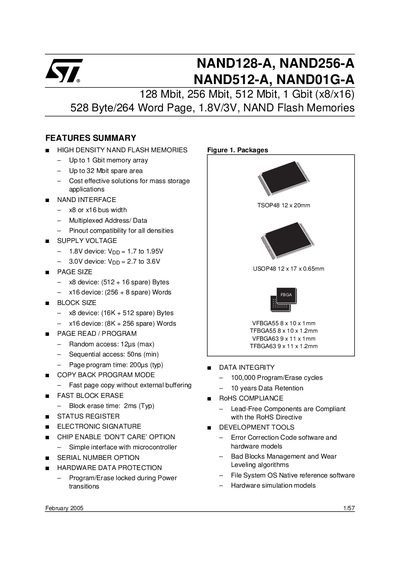
The NAND128-A, NAND256-A, NAND512-A and NANDO1G-A family are high‑density SLC NAND flash memories ranging from 128 Mbit to 1 Gbit. They operate at either 1.8 V or 3 V supply and offer a small‑page architecture with 528 Bytes (512 + 16 spare) per page for x8 devices or 264 Words (256 + 8 spare) for x16 devices.
The devices use a multiplexed x8 or x16 bus, reducing pin count and allowing migration between densities without changing the footprint. They are offered in TSOP48, USOP48, VFBGA55, TFBGA55, VFBGA63 and TFBGA63 packages, provide 100 k program/erase cycles, 10‑year data retention, and include features such as a copy‑back command, open‑drain Ready/Busy output, and optional chip‑enable "don’t‑care" operation.
| Memory densities | 128 Mbit, 256 Mbit, 512 Mbit, 1 Gbit |
|---|---|
| Page size (x16) | 264 Words (256 + 8 spare) |
| Supply voltage (1.8 V devices) | Vpp = 1.7 V to 1.95 V |
| Supply voltage (3.0 V devices) | Vpp = 2.7 V to 3.6 V |
| Typical page program time | 200 µs |
| Typical block erase time | 2 ms |
| Program/Erase endurance | 100 000 cycles |
| Data retention | 10 years |
| Bus width | x8 or x16 |
| Pinout compatibility | All densities share the same pinout |
The family is offered in 128 Mbit, 256 Mbit, 512 Mbit and 1 Gbit densities.
Both 1.8 V (Vpp = 1.7 V – 1.95 V) and 3.0 V (Vpp = 2.7 V – 3.6 V) devices are available.
The typical page program time is 200 µs.
The devices are rated for 100 000 program/erase cycles.