
The STW80NF10 is a low gate charge N-channel MOSFET from STMicroelectronics. It features a typical RDS(on) of 0.012 ohms and excellent dv/dt capability, making it suitable for use in high-efficiency DC-DC converters and UPS and motor control applications.
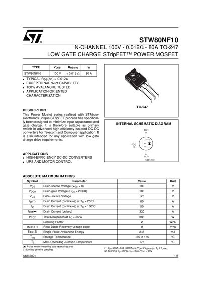
The STW80NF10 is a N‑channel 100 V Power MOSFET realized with STMicroelectronics' STripFET™ process, optimized for low input capacitance and gate charge. It is intended for high‑efficiency DC‑DC converters, UPS, motor control and any application requiring low gate‑drive requirements.
The document provides absolute maximum ratings, thermal data, detailed electrical characteristics, switching performance, source‑drain diode behavior, and mechanical dimensions for the TO‑247 package.
| Drain‑source Voltage (VDS) | 100 V |
|---|---|
| Continuous Drain Current (25 °C) | 80 A |
| Typical On‑Resistance (RDS(on)) | 0.012 Ω |
| Thermal Resistance Junction‑case (RθJC) | 0.5 °C/W |
| Thermal Resistance Junction‑ambient (RθJA) | 62.5 °C/W |
| Total Power Dissipation (25 °C) | 300 W |
| Gate Charge (Qg, typical) | 140 nC |
| Storage Temperature Range | -65 °C to 175 °C |
The STW80NF10 can handle a continuous drain current of 80 A at a case temperature of 25 °C.
Typical on‑resistance is about 0.012 Ω.
The maximum junction‑to‑ambient thermal resistance is 62.5 °C/W.
The device is rated for a maximum drain‑source voltage of 100 V.