
This document describes a triple buffer/driver product with open-drain outputs. It supports 5V VCC operation and features low power consumption, high output drive capability, and ESD protection.
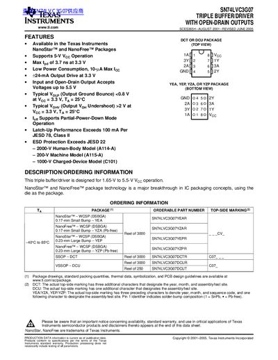
The SN74LVC3G07 is a triple buffer/driver IC with open‑drain outputs that can be used for wired‑OR or wired‑AND functions. It operates from 1.65 V to 5.5 V supply, offers low power consumption, and provides up to 24 mA output drive at 3.3 V. Key electrical characteristics include a typical propagation delay of 3.7 ns and maximum continuous output currents of 50 mA (through VCC) and 100 mA (through GND).
The device is offered in several NanoStar™ and NanoFree™ wafer‑scale packages (WCSP, DCT, DCU) with both lead‑free and tin‑lead options. Mechanical drawings and package dimensions are provided for each option, and the data sheet includes recommended operating conditions, absolute maximum ratings, and detailed switching characteristics.
| Supply voltage range (absolute max) | 0.5 V – 6.5 V |
|---|---|
| Recommended supply voltage | 1.65 V – 5.5 V |
| Maximum output drive current | 24 mA at 3.3 V |
| Typical propagation delay | 3.7 ns at 3.3 V |
| Continuous output current (VCC side) | 50 mA |
| Continuous output current (GND side) | 100 mA |
| Input clamp current | -50 mA |
| Output clamp current | -50 mA |
The device can source up to 24 mA at a 3.3 V supply.
Typical propagation delay is 3.7 ns when powered at 3.3 V.