
MAX4885 is a 1:2 or 2:1 multiplexer for VGA signals from TI. It integrates high-bandwidth analog switches and level-translating buffers, has a low-noise charge pump and internal capacitors, and can provide switching for RGB, DDC and horizontal and vertical synchronization signals. In the 1:2 multiplexer mode, HSYNC/VSYNC inputs feature level-shifting buffers to support low-voltage CMOS or standard TTL-compatible graphics controllers. In the 2:1 multiplexer mode, the output buffers for the HSYNC/VSYNC inputs are disabled, allowing bidirectional signaling. In both modes, DDC signals are voltage-clamped to an external voltage to provide level translation and protection. MAX4885 has a 5µA shutdown mode and is ESD protected to ±8kV Human Body Model (HBM) on externally routed pins. MAX4885 is specified over the extended (-40°C to +85°C) temperature range and is available in the 32-pin, 5mm x 5mm TQFN package.
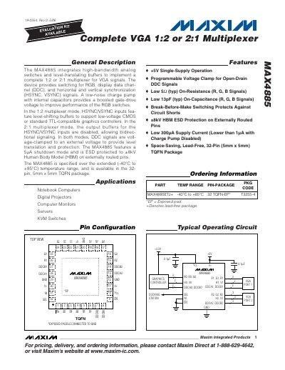
The MAX4885 integrates high‑bandwidth analog switches and level‑translating buffers to provide a complete 1:2 or 2:1 VGA multiplexer. It switches RGB, HSYNC, VSYNC and DDC signals and includes a low‑noise charge pump for boosted gate‑drive voltage.
The device operates from a single 5 V supply, offers ±8 kV HBM ESD protection, and is supplied in a 32‑pin, 5 mm × 5 mm TQFN package. Detailed electrical characteristics, timing diagrams, pin descriptions and layout recommendations are provided for designers.
| Supply Voltage Range | 4.5 V – 5.5 V |
|---|---|
| ESD Protection | ±8 kV Human Body Model |
The device operates from –40 °C to +85 °C.
All pins are protected to ±8 kV HBM.