
The MAX7356/MAX7357/MAX7358 8-channel I2C switches/multiplexers expand the main I2C bus to any combination of 8 extended I2C buses. They enable a master on the main bus to isolate and communicate with devices or groups of devices that may otherwise have slave address conflicts. Any extended bus can be connected or disconnected by control packets from the main I2C bus writing to the main control register of these I2C switches. The MAX7357 and MAX7358 feature an enhanced mode that includes a built-in timer used to monitor all extended buses for lock-up conditions. If the clock or data line of any of these buses is low for more than 25ms (typ), a lock condition is detected. An optional interrupt can be generated through the bidirectional RST/INT. The master can read the bus lock-up register to find out which extended bus is locked up. The mas- ter can also enable the MAX7357 or the MAX7358 to send a “flush-out” sequence on the faulty channel. There is an optional preconnection check that can be enabled to toggle the extended bus clock and data line low then high to ensure the downstream bus is not locked high prior to connecting it to the host bus. The MAX7356/MAX7357/MAX7358 are transparent to signals sent and received at each channel, allowing multiple masters. Any device connected to an I2C bus can transmit and receive signals; however, only the master connected to the host side of the MAX7356/ MAX7357/MAX7358 should address the device.
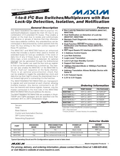
The MAX7356, MAX7357 and MAX7358 are 1‑to‑8 I²C multiplexers that expand a main I²C bus to any combination of eight extended buses. They allow a master to isolate and communicate with devices that may have address conflicts, and provide bus lock‑up detection, isolation, and optional interrupt notification.
The devices are offered in 24‑pin TSSOP and TQFN‑EP packages and operate over a –40 °C to +85 °C temperature range. Electrical specifications include a supply voltage of 2.3 V to 3.6 V (5 V versions also available), typical standby current of 0.1 µA, and a switch resistance of about 55 Ω. Three address control inputs (A0‑A2) select the device address, and an optional RST/INT pin provides reset and interrupt functionality.
| Supply Voltage (VDD) | 2.3 V – 3.6 V |
|---|---|
| Operating Temperature Range | -40 °C to +85 °C |
| Package Types | 24‑pin TSSOP and TQFN‑EP |
| Address Control Inputs | 3 (A0‑A2) |
A lock condition is detected when the clock or data line of any bus stays low for more than 25 ms.
The device provides three address control inputs, labeled A0, A1, and A2.
They are offered in 24‑pin TSSOP and 24‑pin TQFN‑EP (exposed pad) packages.