
The MAX2203 RMS power detector is designed for operation from 800MHz to 2.0GHz. It is suitable for wideband code-division multiple access (WCDMA), cdma2000®, and high-speed downlink/uplink packet access. The device accepts an RF signal at the input and outputs the same voltage regardless of the peak-average of the input signal. The output voltage and input power are linear in dB. The device has a -24dBm to +3dBm detection range, and every dB change in input power gives a 35mV (typ) change in output voltage. The MAX2203 operates from a 2.5V to 4.2V supply and is specified over the -40°C to +85°C extended temperature range. It is available in a 6-bump WLP package.
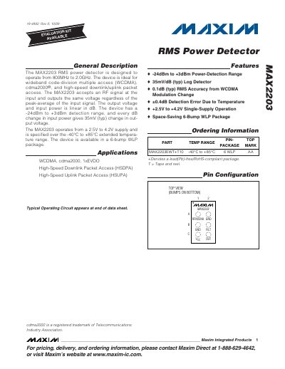
The MAX2203 is a BiCMOS RMS power detector designed for wideband applications such as WCDMA, cdma2000 and high‑speed packet access. It accepts an RF input and provides a voltage output that is linear in dB, independent of the peak‑average of the signal.
The device is supplied in a 6‑bump wafer‑level package, operates from 2.5 V to 4.2 V, and is specified over a temperature range of –40 °C to +85 °C. Typical performance includes a detection range of –24 dBm to +3 dBm, 35 mV/dB conversion, and ±0.4 dB accuracy across temperature.
| Detection Range | -24 dBm to +3 dBm |
|---|---|
| Supply Voltage | 2.5 V to 4.2 V |
| Input Frequency Range | 800 MHz to 2.0 GHz |
| Typical Output Voltage at +3 dBm | 1.05 V – 1.75 V |
| ENA Logic‑High Threshold | 1.1 V |
| ENA Logic‑Low Threshold | 0 V |
| Operating Temperature Range | -40 °C to +85 °C |
The MAX2203 detects input power from –24 dBm up to +3 dBm.
It operates from a single supply of 2.5 V to 4.2 V.
The device is in a 6‑bump wafer‑level package and has six pins.
At +3 dBm input the output voltage is typically between 1.05 V and 1.75 V.