
The MAX4003 is a low-cost, low-power logarithmic amplifier designed to detect the power levels of RF power amplifiers (PAs) operating from 100MHz to 2500MHz. A typical dynamic range of 45dB makes this logarithmic amplifier useful in a variety of wireless applications including cellular handset PA control, TSSI for wireless terminal devices, and other transmitter power measurements. This logarithmic amplifier provides much wider measurement range and superior accuracy than typical diode-based detectors. Excellent temperature stability is achieved over the full operating range of -40°C to +85°C. The MAX4003 logarithmic amplifier is a voltage-measuring device with a typical signal range of -58dBV to -13dBV. The input signal is internally AC-coupled by an on-chip 5pF capacitor in series with a 2kΩ resistor. This highpass coupling, with a corner at 16MHz, sets the lowest operating frequency and allows the input signal source to be DC grounded. The MAX4003 also features a power-on delay, which holds the detector output (OUT) low for approximately 5µs to ensure glitchless controller output. The MAX4003 is available in an 8-bump chip-scale package (UCSP™), an 8-pin µMAX package, and an 8-pin thin QFN package. The device consumes 5.9mA with a 3.0V supply and only 13µA when the device is in shutdown. Applications include cellular handsets (TDMA, CDMA, GPRS, GSM), TSSI for wireless terminal devices, transmitter power measurement and control, and RSSI for fiber modules.
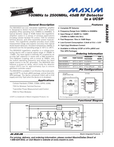
The MAX4003 logarithmic amplifier is designed to detect RF power levels from 100 MHz to 2500 MHz. It offers a typical dynamic range of 45 dB, an input voltage range of –58 dBV to –13 dBV, and excellent temperature stability from –40 °C to +85 °C. The device operates from a 3.0 V supply, drawing 5.9 mA in normal mode and only 13 µA in shutdown.
Available in three package styles (8‑bump UCSP, 8‑pin µMAX, and 8‑pin thin‑QFN), the MAX4003 includes a power‑on delay of about 5 µs to ensure glitch‑free output. Detailed electrical characteristics, noise performance, and typical operating curves are provided for design reference.
| Frequency range | 100 MHz – 2500 MHz |
|---|---|
| Dynamic range | 45 dB |
| Input voltage range | -58 dBV to -13 dBV |
| Supply current (3.0 V) | 5.9 mA |
| Shutdown current | 13 µA (typ) |
| Power‑on delay | ~5 µs |
| Operating temperature range | -40 °C to +85 °C |
| Package options | 8‑bump UCSP, 8‑pin µMAX, 8‑pin thin‑QFN |
The detector output is held low for approximately 5 µs after power‑on.
It draws 5.9 mA when supplied with 3.0 V.
The device operates from –40 °C to +85 °C.
It is offered in 8‑bump UCSP, 8‑pin µMAX, and 8‑pin thin‑QFN packages.