
The MAX9996 is a high-linearity downconversion mixer that provides 8.3dB gain, +26.5dBm IIP3, and 9.7dB NF for 1700MHz to 2200MHz UMTS/WCDMA, DCS, and PCS base-station receiver applications. With a 1900MHz to 2400MHz LO frequency range, this particular mixer is ideal for high-side LO injection receiver architectures. Low-side LO injection is supported by the MAX9994, which is pin-for-pin and functionally compatible with the MAX9996. In addition to offering excellent linearity and noise performance, the MAX9996 also yields a high level of component integration. This device includes a double-balanced passive mixer core, an IF amplifier, a dual-input LO selectable switch, and an LO buffer. On-chip baluns are also integrated to allow for single-ended RF and LO inputs. The MAX9996 requires a nominal LO drive of 0dBm, and supply current is guaranteed to be below 240mA. The MAX9994/MAX9996 are pin compatible with the MAX9984/MAX9986 815MHz to 995MHz mixers, making this entire family of downconverters ideal for applications where a common PC board layout is used for both frequency bands. The MAX9996 is also functionally compatible with the MAX9993. The MAX9996 is available in a compact, 20-pin, thin QFN package (5mm x 5mm) with an exposed paddle. Electrical performance is guaranteed over the extended -40°C to +85°C temperature range. Applications: UMTS/WCDMA Base Stations, DCS1800/PCS1900 EDGE Base Stations, cdmaOne™ and cdma2000® Base Stations, PHS/PAS Base Stations.
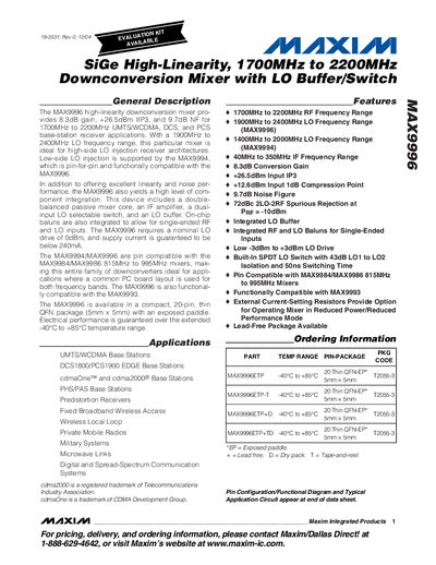
The MAX9996 is a SiGe high‑linearity downconversion mixer designed for 1700‑2200 MHz RF applications such as UMTS/WCDMA, DCS and PCS base‑station receivers. It supports high‑side LO injection with a 1900‑2400 MHz LO range and includes an integrated LO buffer, SPDT switch, and on‑chip baluns for single‑ended RF and LO inputs.
Key specifications include 8.3 dB conversion gain, +26.5 dBm input third‑order intercept point, 9.7 dB noise figure, and a 20‑pin thin QFN‑EP package (5 mm × 5 mm). The device operates over –40 °C to +85 °C and requires a nominal LO drive of –3 dBm to +3 dBm.
| RF Frequency Range | 1700 MHz – 2200 MHz |
|---|---|
| LO Frequency Range | 1900 MHz – 2400 MHz |
| Conversion Gain | 8.3 dB |
| Input IP3 | +26.5 dBm |
| Noise Figure | 9.7 dB |
| Supply Current | 206 mA typical, 240 mA max |
| Package | 20‑pin thin QFN‑EP (5 mm × 5 mm) |
The device requires a nominal LO drive of –3 dBm to +3 dBm.
The maximum supply current is 240 mA, with a typical value of 206 mA.
The exposed pad must be soldered to a ground plane on the PCB, using multiple vias if needed.