
The MAX971–MAX974 and MAX981–MAX984 single/dual/quad low-voltage comparators feature the lowest power consumption available. These micropower devices draw less than 4µA supply current over temperature (MAX971/MAX972/MAX981/MAX982), and include an internal 1.182V ±1% (MAX971/MAX973/ MAX974) or ±2% (MAX981–MAX984) voltage reference and programmable hysteresis. Ideal for 3V or 5V single-supply applications, these devices operate from a single 2.5V to 11V supply (or ±1.25V to ±5.5V dual supplies), and each comparator’s input voltage ranges from the negative supply rail to within 1.3V of the positive supply. The single MAX971/MAX981 and the dual MAX973/ MAX982/MAX983 provide a unique, simple method for adding hysteresis without feedback or complicated equations, simply by using the HYST pin plus two resistors. The MAX971–MAX974 and MAX981–MAX984’s open- drain outputs permit wire-ORed configurations. Thanks to an 11V output range and separate GND pin for the output transistor (MAX971/MAX974, MAX981/MAX984), these devices are ideal for level translators and bipolar to single- ended converters. For similar devices with complementary output stages, see the MAX921–MAX924 (1% reference) and the MAX931–MAX934 (2% reference).
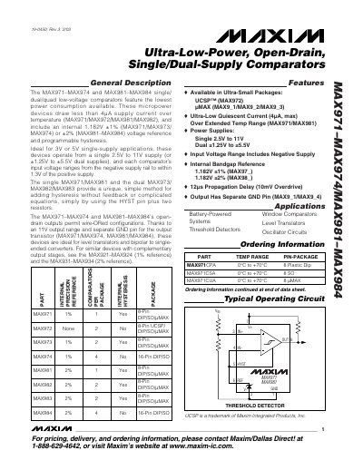
The MAX971–MAX974 and MAX981–MAX984 families are low‑voltage comparators that consume less than 4 µA of supply current and include an internal 1.182 V reference (±1 % for MAX971‑974, ±2 % for MAX981‑984). They operate from a single 2.5 V to 11 V supply or dual ±1.25 V to ±5.5 V supplies, with input voltage range extending from the negative rail to within 1.3 V of the positive rail.
These devices feature open‑drain outputs with a separate GND pin, allowing wire‑OR configurations and making them suitable for level‑translation and bipolar‑to‑single‑ended conversion applications. Typical propagation delay is 12 µs at 10 mV overdrive, and the output voltage can swing from 0 V to 11 V.
| Supply Voltage Range | 2.5 V to 11 V (single) / ±1.25 V to ±5.5 V (dual) |
|---|---|
| Input Voltage Range | V‑ to (V+ ‑ 1.3 V) |
| Reference Voltage | 1.182 V ±1 % (MAX971‑974) or ±2 % (MAX981‑984) |
| Quiescent Current | < 4 µA |
| Output Voltage Range | 0 V to 11 V |
| Propagation Delay (10 mV overdrive) | 12 µs |
| Output Type | Open‑drain with separate GND pin |
| Separate GND Pin | Yes |
They operate from 2.5 V to 11 V with a single supply, or from ±1.25 V to ±5.5 V with dual supplies.
The internal bandgap reference is 1.182 V with ±1 % tolerance for MAX971‑974 and ±2 % for MAX981‑984.
They draw less than 4 µA of supply current over the specified temperature range.
They have open‑drain outputs with a separate GND pin, allowing wire‑OR configurations.