
MAX2691 is a low-noise amplifier from Maxim, which is designed for GPS L2 applications. Designed in Maxim’s advanced SiGe process, the device achieves high gain and low noise figure while maximizing the input-referred 1dB compression point and the 3rd-order intercept point. The MAX2691 provides a high gain of 17.5dB and sub 1dB noise figure. The device operates from a +1.6V to +3.6V single sup- ply. The optional shutdown feature in the device reduces the typical supply current to 4FA. The device is available in a very small, lead-free, RoHS-compliant, 0.86mm x 0.86mm x 0.65mm wafer-level package (WLP).
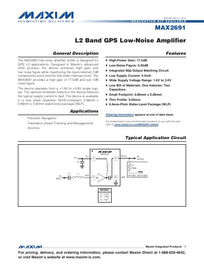
The MAX2691 L2 Band GPS Low‑Noise Amplifier is designed for GPS L2 applications. It is built in Maxim’s SiGe BiCMOS process and offers high gain (up to 17.5 dB) with a sub‑1 dB noise figure while operating from a single‑supply voltage of 1.6 V to 3.6 V. The device includes an optional shutdown pin that reduces typical supply current to about 4 mA.
The amplifier is supplied in a lead‑free, RoHS‑compliant wafer‑level package (0.86 mm × 0.86 mm × 0.65 mm). It requires only an external inductor and DC‑blocking capacitor for input matching, while the output is internally matched to 50 Ω. Typical applications include precision navigation, telematics, and avionics.
| Supply Voltage | 1.6 V to 3.6 V |
|---|---|
| Typical Supply Current (active) | 4.3 mA |
| Typical Supply Current (shutdown) | 20 µA |
| Power Gain (VCC = 2.85 V) | 17.5 dB |
| Noise Figure (VCC = 1.6 V to 3.3 V) | 0.93 dB |
| Input Return Loss | 10.9 dB |
| Output Return Loss | 15.6 dB |
| Package Size | 0.86 mm × 0.86 mm × 0.65 mm (WLP) |
| Operating Temperature Range | -40 °C to +85 °C |
The typical supply current is about 4.3 mA with the shutdown pin high.
It operates from a single supply of 1.6 V to 3.6 V.
The gain is 17.5 dB at VCC = 2.85 V.
It is supplied in a 0.86 mm × 0.86 mm × 0.65 mm wafer‑level package (WLP).