
ADP5023 is a device with two 3 MHz, 800 mA buck regulators and one 300 mA LDO. It has a programmable or externally adjustable output voltage range and is suitable for applications such as processors, ASICs, FPGAs, RF chipsets, portable instrumentation, and medical devices.
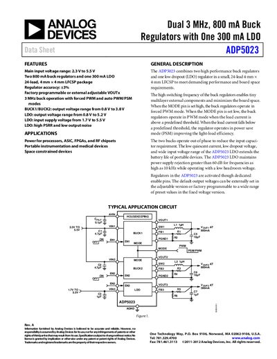
The ADP5023 combines two high‑performance 3 MHz buck regulators and a low‑dropout (LDO) regulator in a compact 24‑lead 4 mm × 4 mm LFCSP package. It offers input voltage ranges of 2.3 V‑5.5 V for the buck converters and 1.7 V‑5.5 V for the LDO, with output voltage ranges of 0.8 V‑3.8 V (buck) and 0.8 V‑5.2 V (LDO). Features include programmable or adjustable output, forced PWM or auto PWM/PSM modes, and high PSRR.
The document provides detailed specifications, pin descriptions, typical application circuits, performance graphs, thermal data, absolute maximum ratings, ordering guide and mechanical dimensions. It serves as a reference for designers integrating the ADP5023 into portable, space‑constrained, or low‑power applications.
| Input voltage range (buck) | 2.3 V to 5.5 V |
|---|---|
| Input voltage range (LDO) | 1.7 V to 5.5 V |
| Output voltage accuracy | ±3 % |
| Buck output voltage range | 0.8 V to 3.8 V |
| LDO output voltage range | 0.8 V to 5.2 V |
| Thermal shutdown threshold | 150 °C |
| Package type | 24‑lead 4 mm × 4 mm LFCSP |
The buck regulators operate from 2.3 V to 5.5 V.
The output voltage accuracy is ±3 % in PWM mode.
Thermal shutdown occurs at a threshold of 150 °C.
It is supplied in a 24‑lead 4 mm × 4 mm LFCSP package.