
The ADP3650 is a dual, high voltage MOSFET driver optimized for driving two N-channel MOSFETs, the two switches in a nonisolated synchronous buck power converter. Each driver is capable of driving a 3000 pF load with a 45 ns propagation delay and a 25 ns transition time. One of the drivers can be bootstrapped and is designed to handle the high voltage slew rate associated with floating high-side gate drivers. The ADP3650 includes overvoltage protection, short-circuit protection, and thermal protection.
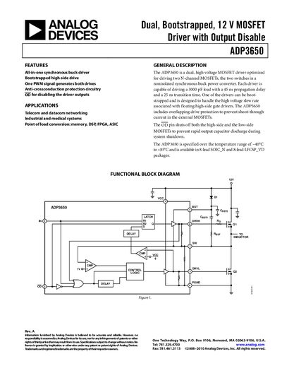
The ADP3650 is a dual, high‑voltage MOSFET driver optimized for driving two N‑channel MOSFETs in non‑isolated synchronous buck converters. It features a bootstrapped high‑side drive, a single PWM input, anti‑cross‑conduction protection, and an output‑disable (OD) pin that shuts off both MOSFETs.
The device is supplied in 8‑lead SOIC_N and 8‑lead LFCSP_VD packages, operates from –40 °C to +85 °C, and supports load capacitances up to 3000 pF with propagation delays as low as 45 ns. Detailed specifications, pin functions, timing diagrams, thermal data, and PCB layout guidelines are provided.
| Input Voltage High | 2.0 V |
|---|---|
| Input Voltage Low | 0.8 V |
| High‑Side Driver Output Resistance (sourcing, 25 °C) | 3.3 Ω |
| Supply Voltage Range | 4.15 V to 13.2 V |
| Operating Ambient Temperature Range | –40 °C to +85 °C |
| Package Types | 8‑Lead SOIC_N, 8‑Lead LFCSP_VD |
The OD pin shuts off both the high‑side and low‑side MOSFETs to prevent rapid output capacitor discharge during system shutdown.
The ADP3650 is offered in 8‑Lead SOIC_N (R‑8) and 8‑Lead LFCSP_VD (CP‑8‑2) packages.
The high input voltage level is specified as 2.0 V.