
The GS4915 is a low jitter clock output chip launched by Gennum. It can reduce jitter for clocks of 148.5MHz, 148.5/1.001MHz, 74.25MHz, 74.25/1.001MHz and 27MHz. The output jitter is as low as 20ps peak to peak, and it can automatically bypass other clock frequencies. In addition, the GS4915 supports single-ended and differential inputs, and has single-ended and differential outputs. It supports LVCMOS and LVDS interfaces and can be widely used in high-definition video systems, digital video recording, playback, processing, and display devices.
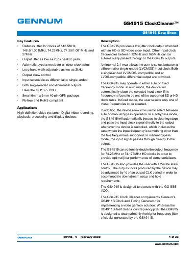
The GS4915 Clock Cleaner provides low‑jitter clock output for HD and SD video systems, supporting input frequencies of 148.5 MHz, 148.5/1.001 MHz, 74.25 MHz, 74.25/1.001 MHz and 27 MHz. It offers automatic and manual bypass modes, selectable differential or single‑ended inputs, and both differential and single‑ended outputs in a compact 6 mm × 6 mm 40‑pin QFN package.
The data sheet includes detailed pin descriptions, electrical characteristics (DC and AC), package dimensions, recommended PCB footprint, and reference standards. Key performance figures such as output jitter as low as 20 ps peak‑to‑peak, loop bandwidth down to 2 kHz, and output skew control are provided, along with typical power consumption and operating temperature ranges. This manual is written in Chinese.
| Supported input clock frequencies | 148.5 MHz, 148.5/1.001 MHz, 74.25 MHz, 74.25/1.001 MHz, 27 MHz |
|---|---|
| Output jitter (peak‑to‑peak) | 20 ps |
| Loop bandwidth (minimum) | 2 kHz |
| Output skew control | Enabled (2‑state) |
| Input selection | Differential or single‑ended |
| Output types | Differential and single‑ended |
| Package | 6 mm × 6 mm 40‑pin QFN |
| Operating temperature range | -20 °C to 85 °C |
It supports 148.5 MHz, 148.5/1.001 MHz, 74.25 MHz, 74.25/1.001 MHz and 27 MHz video clock inputs.
The device offers automatic bypass, which activates when the input frequency is unsupported or the device is unlocked, and manual bypass, which passes the input directly to the output.
The GS4915 is supplied in a 6 mm × 6 mm 40‑pin QFN package.
The cleaned output jitter can be as low as 20 ps peak‑to‑peak.