
This document describes the features and characteristics of the MRF1513NT1 RF power field effect transistor. The transistor is designed for broadband commercial and industrial applications with frequencies up to 520 MHz. The high gain and broadband performance of this device make it ideal for large-signal, common source amplifier applications in 7.5 volt portable and 12.5 volt mobile FM equipment. At 520 MHz and 12.5 volts, the transistor has an output power of 3 watts, power gain of 11 dB, and efficiency of 55%. It is capable of handling a 20:1 VSWR and has excellent thermal stability. The transistor is characterized with series equivalent large-signal impedance parameters. The N suffix indicates lead-free terminations and it is RoHS compliant. It is available in tape and reel packaging.
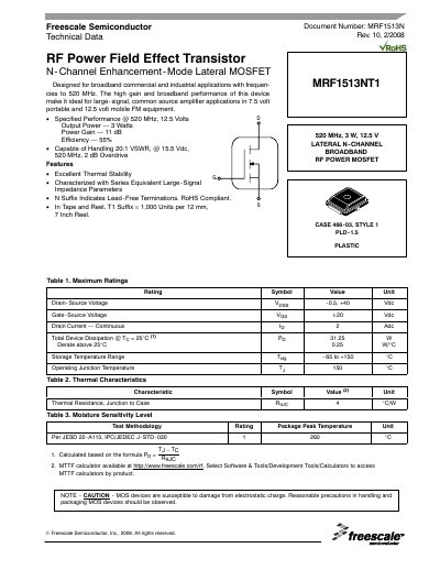
The MRF1513NT1 is a broadband N‑channel enhancement‑mode lateral MOSFET designed for commercial and industrial RF applications up to 520 MHz. It delivers up to 3 W output power at 12.5 V with 11 dB gain and 55 % drain efficiency, and can handle a 20:1 VSWR.
Typical uses include large‑signal common‑source amplifiers in portable 7.5 V and mobile 12.5 V FM equipment. The device is supplied in a lead‑free, RoHS‑compliant PLD‑1.5 plastic package, available in tape‑and‑reel form for automated assembly.
| Maximum Frequency | 520 MHz |
|---|---|
| Output Power | 3 W |
| Power Gain | 11 dB |
| Drain Efficiency | 55 % |
| Drain‑Source Voltage (VDSS) | -0.5 V to +40 V |
| Gate‑Source Voltage (VGS) | ±20 V |
| Thermal Resistance (RθJC) | 4 °C/W |
The device can deliver up to 3 W of output power at 520 MHz and 12.5 V.
It achieves a drain efficiency of about 55 %.
The specified thermal resistance is 4 °C/W.
It is supplied in a lead‑free tape‑and‑reel format, 1,000 units per 12 mm reel.