
This document describes the features and characteristics of MicroConverter, 12-Bit ADCs and DACs with Embedded 62 kB Flash MCU ADuC832 Rev. A, including 8-channel, 247 kSPS, 12-bit ADC, 2 12-bit voltage output DACs, dual output PWM/Σ-Δ DACs, etc.
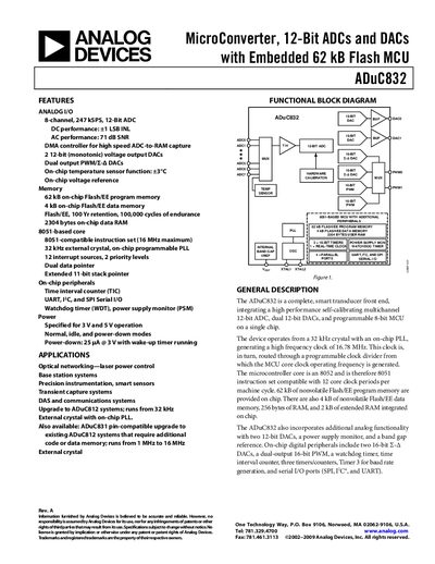
The ADuC832 is a 12‑bit microcontroller with integrated ADC, dual DACs, flash memory, and a range of on‑chip peripherals. It operates from 3 V or 5 V and includes a PLL‑generated 16.78 MHz core clock, power‑down mode with 25 pA consumption, and extensive serial interfaces.
The handbook covers functional block diagrams, detailed pin configurations, timing specifications, memory organization, and programming information. It also includes application notes for optical networking, precision instrumentation, and sensor integration, as well as hardware design considerations such as power supply monitoring and watchdog timer usage.
| Power‑down current | 25 pA @ 3 V |
|---|---|
| Flash program memory | 62 kB |
| Flash data memory | 4 kB |
| Maximum core clock | 16.78 MHz |
The device can run up to 16.78 MHz, programmable via the PLL.
It includes 62 kB of on‑chip flash program memory.
In power‑down mode the part draws 25 pA at 3 V.