
This document introduces the features and characteristics of ADSP-BF535.
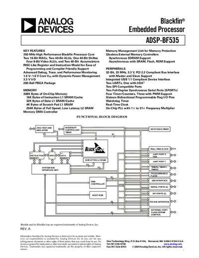
The ADSP‑BF535 is a 350 MHz Blackfin® embedded processor featuring two 16‑bit MACs, multiple ALUs, and extensive on‑chip memory. It supports dynamic power management, a 1.0 V‑1.6 V core voltage range, and a 260‑ball PBGA package. The handbook details the processor’s functional blocks, including UARTs, SPI ports, SPORTs, timers, watchdog, real‑time clock, and PCI/USB interfaces.
Memory is organized in a hierarchical structure with 308 KB of on‑chip memory (16 KB L1 instruction SRAM, 32 KB L1 data SRAM, 4 KB scratch‑pad SRAM, 256 KB L2 SRAM) and support for external SDRAM, flash, and SRAM via the External Bus Interface Unit. The document also describes boot modes, event handling, and PCI bus integration for system design.
| Core frequency | 350 MHz |
|---|---|
| Package type | 260‑Ball PBGA |
| Core voltage range | 1.0 V‑1.6 V |
| On‑chip memory total | 308 KB |
| L1 instruction SRAM | 16 KB |
| L1 data SRAM | 32 KB |
| L2 SRAM | 256 KB |
| UART ports | Two (one with IrDA) |
| SPI ports | Two |
| SPORT ports | Two Full‑Duplex |
| Timers with PWM | Four (three with PWM support) |
The ADSP‑BF535 processor runs at 350 MHz.
It provides 308 KB of on‑chip memory, consisting of 16 KB L1 instruction SRAM, 32 KB L1 data SRAM, 4 KB scratch‑pad SRAM, and 256 KB L2 SRAM.